

Semiconductor
Industry
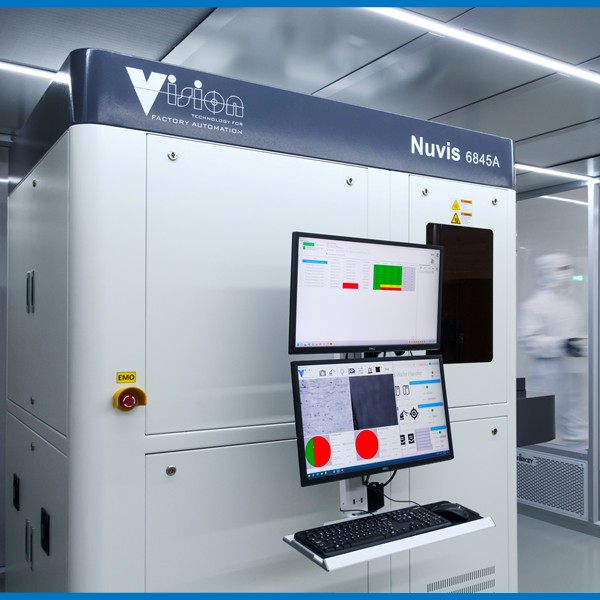

Photoluminescence Mapping System
With its unique optical design technology, the System detects and classifies defects that affect yield and uses advanced photoluminescence (PL) technology to enable real-time monitoring of MOCVD production processes.
NUV-PL SiC Defect Inspection System
Comply with IEC63068-3 Standard:
Test method for defects using photoluminescence, Model VS-6845 SiC Wafer defect inspection system has capability on Non-destructive recognition criteria of defects in silicon carbide homoepitaxial wafer for power devices.